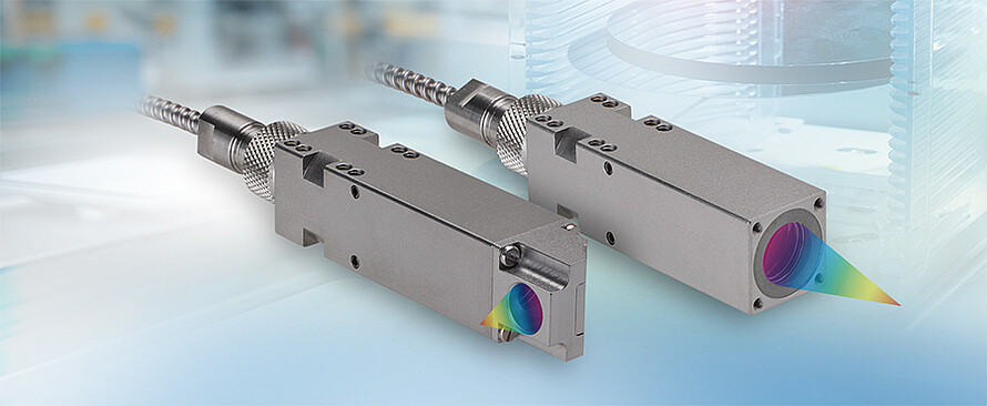
confocalDT IFS2407-xHT/VAC -korkean lämpötilan anturit asettavat uudet standardit vaativissa ympäristöissä tehtäville mittauksille. Konfokaaliset anturit tuottavat erittäin tarkkoja mittaustuloksia jopa 200 °C:n lämpötiloissa. Minimaalisen…
OptoCONTROL 2700 -tarkkuusmikrometri pystyy nyt suorittamaan pyörivien komponenttien täyden 360° tarkastuksen. Tämä mahdollistaa neljän muoto- ja sijaintitoleranssin tarkan määrittämisen ja visualisoinnin ympyrädiagrammissa: pyöreys, heitto,…

Micro-Epsilonin capaNCDT-sarja tarjoaa maailman edistyneimmän kapasitiivisten antureiden tuotevalikoiman. Nämä anturit mittaavat siirtymää, etäisyyttä ja sijaintia teollisuusympäristöissä mittausalueilla 50 µm - 10 mm. Korkean tarkkuuden (jopa 0,03…
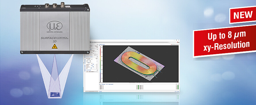
Micro-Epsilon asettaa uudet standardit mattapintaisten kohteiden geometrian, muodon ja pinnan tarkastukseen surfaceCONTROL 3D –snapshot antureilla. Uusimman sukupolven anturit tarjoavat Z-akselin toistettavuuden 0,25 mikrometriä ja XY-resoluutiota…